


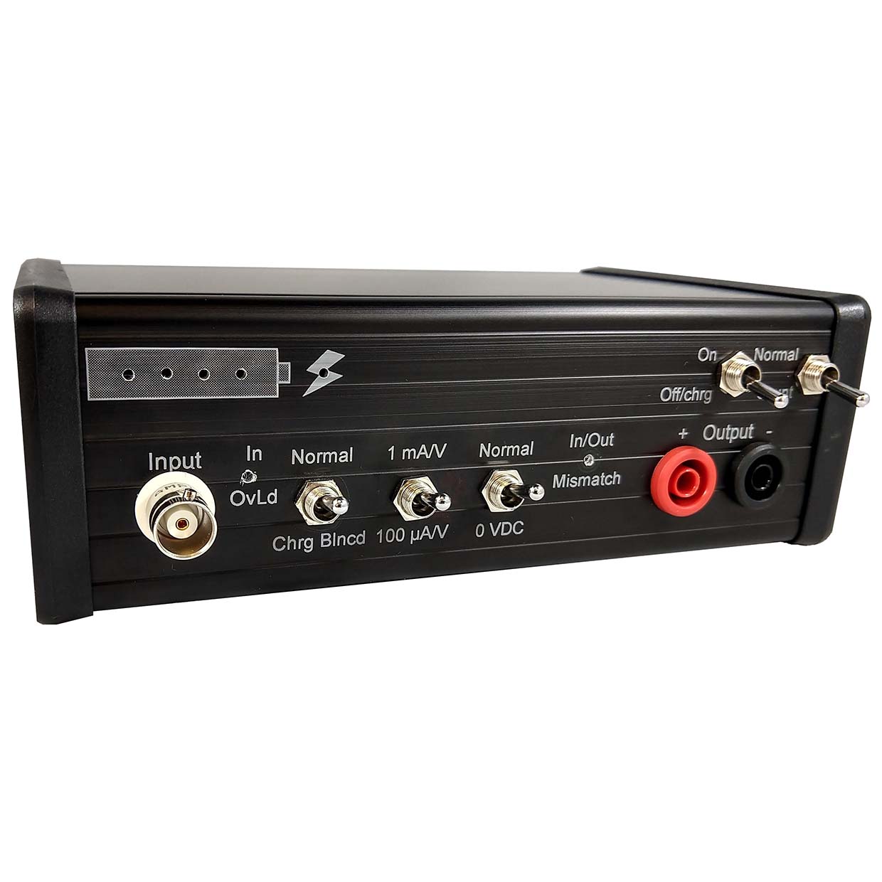

High Voltage Linear Current Isolator
 90 Day Hassle Free Returns
 Free Shipping on Orders Over $50

About This Product


Need to Return Your Purchase? It's Easy - Caputron Offers 90 Day Hassle Free Returns
Our return policy is simple. If you are not 100% satisfied with your purchase from Caputron you can return your item(s) within 90 days of purchase. If 90 days have gone by since your purchase, unfortunately we can’t offer you a refund or exchange.
Returned devices must be in a like-new and undamaged condition. Products returned damaged may not qualify for a refund.
Opened or used accessories such as electrodes, gel, saline, head straps, or other consumables are not eligible for a refund.
Shipping
--------
Orders are generally dispatched within 1-3 days after receipt of payment, though some exceptions may apply, and
are shipped via UPS, DHL and USPS with tracking (when applicable) and drop-off without signature. If you prefer
delivery by a different method, please contact us. Delivery with signature is available for an additional fee.
Once your order is shipped you will receive an email or sms message when applicable (additional carrier rates may apply) with any tracking information available -- you can check order status by logging into your account.
International Customers Please Note: Any additional fees required by customs will be the responsibility of the buyer. We cannot control customs processing times in international countries.
It is not uncommon for USPS First Class/Flat Rate parcels, or packages of any type, to get caught up in customs for weeks at a time. We highly recommend using UPS or DHL for international orders as they provide faster customs processing times and accurate tracking updates.
We are not responsible for any added time due to customs. We will not be liable for, nor will any adjustment, refund, or credit of any kind be given as a result of any delay, misdelivery, or non-delivery. Items returned to us that were deemed undeliverable and are not damaged in any way are subject to partial refund for the cost of the merchandise minus the cost of shipping.
At the discretion of both Caputron and the buyer, redelivery may be attempted for additional shipping costs determined prior to reshipment.
* When offered, free shipping is eligible only for the contiguous United States and does not apply to items that need to be shipped freight or for certain research items.
